BASIC CIRCUIT -THAT MAKES 8051 WORKS
EA/VP Pin
The EA on pin 31 is tied high to make the 8051 executes program from Internal ROM
Reset Circuit
RESET is an active High input When RESET is set to High, 8051 goes back to the power on state.
The 8051 is reset by holding the RST high for at least two machine cycles and then returning it low.
Power-On Reset
- Initially charging of capacitor makes RST High
- When capacitor charges fully it blocks DC.
Manual reset
-closing the switch momentarily will make RST High.
After a reset, the program counter is loaded with 0000H but the content of on-chip RAM is not affected.
| Register | Content | Register | Content |
Program counter
|
0000h
| IP |
XXX00000b
|
Accumulator
|
00h
| IEv | 0XX00000b |
B register
|
00h
| All timer registers | 00h |
PSW
|
00h
| SCON | 00h |
SP
|
07h
| SBUF | 00h |
DPTR
|
0000h
| PCON (HMOS) | 0XXXXXXXbv |
All ports
|
FFh
| PCON (CMOS)v | 0XXX0000b |
Note: content of on-chip RAM is not affected by Reset.
Oscillator Circuit
The 8051 uses the crystal for precisely that: to synchronize it’s operation. Effectively, the 8051 operates using what are called "machine cycles." A single machine cycle is the minimum amount of time in which a single 8051 instruction can be executed. although many instructions take multiple cycles. 
8051 has an on-chip oscillator. It needs an external crystal thats decides the operating frequency of the 8051.
This can be achieved in two ways,,
The crystal is connected to pins 18 and 19 with stabilizing capacitors. 12 MHz(11.059MHz) crystal is often used and the capacitance ranges from 20pF to 40pF.
The oscillator can also be a TTL clock source connected with a NOT gate asshown
How fast 8051 works ?
A cycle is, in reality, 12 pulses of the crystal. That is to say, if an instruction takes one machine cycle to execute, it will take 12 pulses of the crystal to execute. Since we know the crystal is pulsing 11,059,000 times per second and that one machine cycle is 12 pulses, we can calculate how many instruction cycles the 8051 can execute per second:
11,059,000 / 12 = 921,583
Why is such an oddball crystal frequency?
11.0592 MHz crystals are often used because it can be divided to give you exact clock rates for most of the common baud rates for the UART, especially for the higher speeds (9600, 19200). Despite the "oddball" value, these crystals are readily available and commonly used.
Power Supply
C1-1000 mf
,C2-100 mf
The 78L05 is a 5V regulator. The input voltage ranges from 7V to 35V and the output voltage is about 5V.
Using Ports for I/O Operation
8051 is TTL logic device. TTL logic has two levels: Logic "High" (1) and logic "Low" (0). The voltage and current involved for the two levels are as follows:
Level
|
Voltage
| Current |
| High | Above 2.4V | Virtually no current flow |
| Low | Below 0.9V | 1.6mA Sinking current from TTL input to ground
(Depends on logic family) |
Port functions
Ports
|
Function
|
Port 0
(Pin 32-39)
|
Dual-purpose port- 1. general purpose I/O Port.
2. multiplexed address & data bus
Open drain outputs
|
Port 1
(Pin 1-8)
|
Dedicated I/O port – Used solely for interfacing to external devices
Internal pull-ups
|
Port 2
(Pin 21-28)
|
Dual-purpose port- 1. general purpose I/O port.
2. a multiplexed address & data bus.
Internal pull-ups
|
Port 3
(Pin 10-17)
|
Dual-purpose port- 1. general purpose I/O port.
2. pins have alternate purpose related to special features of the 8051
Internal pull-ups
|
The 8051 internal ports are partly bi-directional (Quasi-bi-directional). The following is the internal circuitry for the 8051 port pins:
1.Configuring for output
P0 is open drain.
– Has to be pulled high by external 10K resistors.
– Not needed if P0 is used for address lines
Writing to a port pin loads data into a port latch that drives a FET connected to the port pin.
P0: Note that the pull-up is absent on Port 0 except when functioning as the external address/data bus. When a "0" is written to a bit in port 0, the pin is pulled low. But when a "1" is written to it, it is in high impedance (disconnected) state. So when using port 0 for output, an external pull-up resistor is needed, depending on the input characteristics of the device driven by the port pin
P1, P2, P3 have internal pull-ups: When a "0" is written to a bit in these port , the pin is pulled low ( FET-ON) ,also when 1 is written to a bit in these port pin becomes high (FET-OFF) thus using port P1,P2,P3 is simple.
2. Configuring for input
At power-on all are output ports by default
To configure any port for input, write all 1’s (0xFF) to the port
Latch bit=1, FET=OFF, Read Pin asserted by read instruction
You can used a port for output any time. But for input, the FET must be off. Otherwise, you will be reading your own latch rather than the signal coming from the outside. Therefore, a "1" should be written to the pin if you want to use it as input, especially when you have used it for output before. If you don't do this input high voltage will get grounded through FET so you will read pin as low and not as high. An external device cannot easily drive it high
so, you sh ould not tide a port high directly without any resistor. Otherwise, the FET would burn.
LED INTERFACING WITH 8051
LED:
Light emitting diodes (LEDs) are semiconductor light sources. The light emitted from LEDs varies from visible to infrared and ultraviolet regions. They operate on low voltage and power. LEDs are one of the most common electronic components and are mostly used as indicators in circuits. They are also used for luminance and optoelectronic applications.
Based on semiconductor diode, LEDs emit photons when electrons recombine with holes on forward biasing. The two terminals of LEDs are anode (+) and cathode (-) and can be identified by their size. The longer leg is the positive terminal or anode and shorter one is negative terminal.
The forward voltage of LED (1.7V-2.2V) is lower than the voltage supplied (5V) to drive it in a circuit. Using an LED as such would burn it because a high current would destroy its p-n gate. Therefore a current limiting resistor is used in series with LED. Without this resistor, either low input voltage (equal to forward voltage) or PWM (pulse width modulation) is used to drive the LED.
LEDs are by far the most widely used means of taking output. They find huge application as indicators during experimentations to check the validity of results at different stages. They are very cheap and easily available in a variety of shape, size and colors.
The principle of operation of LEDs is simple. The commonly available LEDs have a drop voltage of 1.7 V and need 10 mA to glow at full intensity. The following circuit describes “how to glow an led”.
The value of resistance R can be calculated using the equation, R= (V-1.7)/10 mA. Since most of the controllers work on 5V, so substituting V= 5V, the value of resistance comes out to be 330 ohm. The resistance 220 ohm, 470 ohm is commonly used substitute in case 330 ohm is not available.
AT89C51 is a 40 pin microcontroller which belongs to 8051 series of microcontroller. It has four ports each of 8 bits P0, P1, P2 and P3.The AT89C51 has 4K bytes of programmable flash. The port P0 covers the pin 32 to pin 39, the port P1 covers the pin 1 to pin 8, the port P2 covers the pin 21 to pin 28 and the port P3 covers the pin 10 to pin 17. Pin 9 is the reset pin. The reset is active high. Whenever the controller is given supply, the reset pin must be given a high signal to reset the controller and bring the program counter to the starting address 0x0000. The controller can be reset by manually connecting a switch or by connecting a combination of resistor and capacitor as shown in the circuit diagram. A 12 MHz crystal is connected between pin 18 pin 19. Pin 40 is Vcc and pin 20 is ground. Pin 31, is connected to Vcc as we are using the internal memory of the controller.
LEDs are connected to the port P0. LEDs need approximately 10mA current to flow through them in order to glow at maximum intensity. However the output of the controller is not sufficient enough to drive the LEDs, so if the positive leg of the LED is connected to the pin and the negative to ground as shown in the figure, the LED will not glow at full illumination.
To overcome this problem LEDs are connected in the reverse order and they run on negative logic i.e., whenever 1 is given on any pin of the port, the LED will switch off and when logic 0 is provided the LED will glow at full intensity.
As soon as we provide supply to the controller, the LEDs start blinking i.e., they become on for a certain time duration and then become off for the same time duration. This delay is provided by calling the delay function. The values inside the delay function have been set to provide a delay in multiples of millisecond (delay (100) will provide a delay of 100 millisecond).
7 SEGMENT DISPLAY INTERFACING WITH 8051

INTRODUCTION
For the seven segment display you can use the LT-541 or LSD5061-11 chip. Each of the segments of the display is connected to a pin on the 8051 (the schematic shows how to do this). In order to light up a segment on the the pin must be set to 0V. To turn a segment off the corresponding pin must be set to 5V. This is simply done by setting the pins on the 8051 to '1' or '0'.
LED displays are
But they are cheaper than LCD display
7-SEG Display are available in two types -1. Common anode & 2. common cathode , but command anode display are most suitable for interfacing with 8051 since 8051 port pins can sink current better than sourcing it.
CREATING DIGIT PATTERN
For displaying Digit say 7 we need to light segments -a ,b, c. Since we are using Common anode display , to do so we have to to provide Logic -0 (0 v) at anode of these segments.
so need to clear pins- P1.0 ,P1.1,P1.2. that is 1 1 1 1 1 0 0 0 -->F8h
Connections
Segment number
|
8051 pin number
|
a
|
P1.0
|
b
|
P1.1
|
c
|
P1.2
|
d
|
P1.3
|
e
|
P1.4
|
f
|
P1.5
|
g
|
p1.6
|
h(dp)
|
P1.7
|
Hex Code
Digit
|
Seg. h
|
Seg. g
|
Seg. f
|
Seg. e
|
Seg. d
|
Seg. c
|
Seg. b
|
Seg. a
|
HEX
|
0
|
1
|
1
|
0
|
0
|
0
|
0
|
0
|
0
|
C0
|
1
|
0
|
0
|
0
|
0
|
0
|
1
|
1
|
0
|
06
|
2
|
1
|
0
|
1
|
0
|
0
|
1
|
0
|
0
|
A4
|
3
|
1
|
0
|
1
|
1
|
0
|
0
|
0
|
0
|
B0
|
4
|
1
|
0
|
0
|
1
|
1
|
0
|
0
|
1
|
99
|
You can also do this for some characters like A ,E .. but not for D or B because it will be same as that of 0 & 8 . So this is one of limitation of 7-seg display.
Since we can Enable only one 7-seg display at a time ,we need to scan these display at fast rate .The scanning frequency should be high enough to be flicker-free. At least 30HZ .Therefore – time one digit is ON is 1/30 seconds
INTERFACING
Note that I am using Common Anode display. so the common Anode pin is tied to 5v .The cathode pins are connected to port 1 through 330 Ohm resistance (current limiting).
Common Anode display
CODE EXAMPLE
Connection - a:h to port p1.0:p1.7 , D0:D1 to p3.0:p3.1.
To Display - Consider example of vending machine where we want to display number of soft drink bottles on display entered by customer. Suppose he enter 3 (03) bottles then we will use lookup table to see DIGIT PATTERN of these keys.
So DIGI[1]=c0 (hex code for '0') &
DIGI[2]=bo(hex code for '3').
Note: I have taken values for DIGI[1] & DIGI[2] directly in code.
Algorithm
start : disable [D0:D1]
again : enable D0
[a:h] - pattern for Digit1
delay
disable D0. Enable D1
[a:h] - pattern for Digit2
delay
Goto again
C LANGUAGE
#include <Intel\8052.h>
#include <standard.h>
#include<stdio.h>
#include<etc.h>
void main( ){
unsigned char DIGI[2];
unsigned char right,cnt;
P1 = 0; /* initialize all P1 outputs to be zero*/
P3 = 0;
DIGI[1]=0xc0;/*(hex code for '0')*/
DIGI[2]=0xb0;/*(hex code for '3')*/
while(1) {
for (cnt=1;cnt<3;cnt++)
{
P3 = cnt; /*Enable D0 and then D1*/
P1=DIGI[cnt];/*P1=c0 when D0 is enabled & P1=b0 when d1 is enabled*/
delay_ms(20);
}
}
}
LCD INTERFACING WITH 8051
LCD INTRODUCTION
The most commonly used Character based LCDs are based on Hitachi's HD44780 controller or other which are compatible with HD44580. In this tutorial, we will discuss about character based LCDs, their interfacing with various microcontrollers, various interfaces (8-bit/4-bit), programming, special stuff and tricks you can do with these simple looking LCDs which can give a new look to your application.
For Specs and technical information HD44780 controller Click Here
PIN DESCRIPTION
The most commonly used LCDs found in the market today are 1 Line, 2 Line or 4 Line LCDs which have only 1 controller and support at most of 80 characters, whereas LCDs supporting more than 80 characters make use of 2 HD44780 controllers.
Most LCDs with 1 controller has 14 Pins and LCDs with 2 controller has 16 Pins (two pins are extra in both for back-light LED connections). Pin description is shown in the table below.
| Pin no. 1 | VSS | Power supply (GND) |
| Pin no. 2 | VCC | Power supply (+5V) |
| Pin no. 3 | VEE | Contrast adjust |
| Pin no. 4 | RS | 0 = Instruction input
1 = Data input |
| Pin no. 5 | R/W | 0 = Write to LCD module
1 = Read from LCD module |
| Pin no. 6 | EN | Enable signal |
| Pin no. 7 | D0 | Data bus line 0 (LSB) |
| Pin no. 8 | D1 | Data bus line 1 |
| Pin no. 9 | D2 | Data bus line 2 |
| Pin no. 10 | D3 | Data bus line 3 |
| Pin no. 11 | D4 | Data bus line 4 |
| Pin no. 12 | D5 | Data bus line 5 |
| Pin no. 13 | D6 | Data bus line 6 |
| Pin no. 14 | D7 | Data bus line 7 (MSB) |
Table 1: Character LCD pins with 1 Controller
| Pin no. 1 | D7 | Data bus line 7 (MSB) |
| Pin no. 2 | D6 | Data bus line 6 |
| Pin no. 3 | D5 | Data bus line 5 |
| Pin no. 4 | D4 | Data bus line 4 |
| Pin no. 5 | D3 | Data bus line 3 |
| Pin no. 6 | D2 | Data bus line 2 |
| Pin no. 7 | D1 | Data bus line 1 |
| Pin no. 8 | D0 | Data bus line 0 (LSB) |
| Pin no. 9 | EN1 | Enable signal for row 0 and 1 (1stcontroller) |
| Pin no. 10 | R/W | 0 = Write to LCD module
1 = Read from LCD module |
| Pin no. 11 | RS | 0 = Instruction input
1 = Data input |
| Pin no. 12 | VEE | Contrast adjust |
| Pin no. 13 | VSS | Power supply (GND) |
| Pin no. 14 | VCC | Power supply (+5V) |
| Pin no. 15 | EN2 | Enable signal for row 2 and 3 (2ndcontroller) |
| Pin no. 16 | NC | Not Connected |
Table 2: Character LCD pins with 2 Controller
Usually these days you will find single controller LCD modules are used more in the market. So in the tutorial we will discuss more about the single controller LCD, the operation and everything else is same for the double controller too. Lets take a look at the basic information which is there in every LCD.
DDRAM- DISPLAY DATA RAM
Display data RAM (DDRAM) stores display data represented in 8-bit character codes. Its extended capacity is 80 X 8 bits, or 80 characters. The area in display data RAM (DDRAM) that is not used for display can be used as general data RAM. So whatever you send on the DDRAM is actually displayed on the LCD. For LCDs like 1x16, only 16 characters are visible, so whatever you write after 16 chars is written in DDRAM but is not visible to the user.
Figures below will show you the DDRAM addresses of 1 Line, 2 Line and 4 Line LCDs.
DDRAM Address for 1 Line LCD
DDRAM Address for 2 Line LCD
DDRAM Address for 4 Line LCD
CGROM-CHARACTER GENERATOR ROM
Now you might be thinking that when you send an ascii value to DDRAM, how the character is displayed on LCD? so the answer is CGROM. The character generator ROM generates 5 x 8 dot or 5 x 10 dot character patterns from 8-bit character codes (see Figure 5 and Figure 6 for more details). It can generate 208 5 x 8 dot character patterns and 32 5 x 10 dot character patterns. Userdefined character patterns are also available by mask-programmed ROM.
LCD characters code map for 5x8 dots
LCD characters code map for 5x10 dots
As you can see in both the code maps, the character code from 0x00 to 0x07 is occupied by the CGRAM characters or the user defined characters. If user want to display the fourth custom character then the code to display it is 0x03 i.e. when user send 0x03 code to the LCD DDRAM then the fourth user created charater or patteren will be displayed on the LCD.
CGRAM-CHARACTER GENERATOR RAM
As clear from the name, CGRAM area is used to create custom characters in LCD. In the character generator RAM, the user can rewrite character patterns by program. For 5 x 8 dots, eight character patterns can be written, and for 5 x 10 dots, four character patterns can be written. Later in this tutorial i will explain how to use CGRAM area to make custom character and also making animations to give nice effects to your application.
BF-BUSY FLAG
Busy Flag is an status indicator flag for LCD. When we send a command or data to the LCD for processing, this flag is set (i.e BF =1) and as soon as the instruction is executed successfully this flag is cleared (BF = 0). This is helpful in producing and exact ammount of delay. for the LCD processing.
To read Busy Flag, the condition RS = 0 and R/W = 1 must be met and The MSB of the LCD data bus (D7) act as busy flag. When BF = 1 means LCD is busy and will not accept next command or data and BF = 0 means LCD is ready for the next command or data to process.
INSTRUCTION REGISTER(IR) & DATA REGISTER(DR)
There are two 8-bit registers in HD44780 controller Instruction and Data register. Instruction register corresponds to the register where you send commands to LCD e.g LCD shift command, LCD clear, LCD address etc. and Data register is used for storing data which is to be displayed on LCD. when send the enable signal of the LCD is asserted, the data on the pins is latched in to the data register and data is then moved automatically to the DDRAM and hence is displayed on the LCD.
Data Register is not only used for sending data to DDRAM but also for CGRAM, the address where you want to send the data, is decided by the instruction you send to LCD. We will discuss more on LCD instuction set further in this tutorial.
COMMANDS & INSTRUCTION SET
Only the instruction register (IR) and the data register (DR) of the LCD can be controlled by the MCU. Before starting the internal operation of the LCD, control information is temporarily stored into these registers to allow interfacing with various MCUs, which operate at different speeds, or various peripheral control devices. The internal operation of the LCD is determined by signals sent from the MCU. These signals, which include register selection signal (RS), read/write signal (R/W), and the data bus (DB0 to DB7), make up the LCD instructions (Table 3). There are four categories of instructions that:
- Designate LCD functions, such as display format, data length, etc.
- Set internal RAM addresses
- Perform data transfer with internal RAM
- Perform miscellaneous functions
Command and Instruction set for LCD type HD44780

Although looking at the table you can make your own commands and test them. Below is a breif list of useful commands which are used frequently while working on the LCD.
| 1 | Function Set: 8-bit, 1 Line, 5x7 Dots | 0x30 | 48 |
| 2 | Function Set: 8-bit, 2 Line, 5x7 Dots | 0x38 | 56 |
| 3 | Function Set: 4-bit, 1 Line, 5x7 Dots | 0x20 | 32 |
| 4 | Function Set: 4-bit, 2 Line, 5x7 Dots | 0x28 | 40 |
| 5 | Entry Mode | 0x06 | 6 |
| 6 | Display off Cursor off
(clearing display without clearing DDRAM content) | 0x08 | 8 |
| 7 | Display on Cursor on | 0x0E | 14 |
| 8 | Display on Cursor off | 0x0C | 12 |
| 9 | Display on Cursor blinking | 0x0F | 15 |
| 10 | Shift entire display left | 0x18 | 24 |
| 12 | Shift entire display right | 0x1C | 30 |
| 13 | Move cursor left by one character | 0x10 | 16 |
| 14 | Move cursor right by one character | 0x14 | 20 |
| 15 | Clear Display (also clear DDRAM content) | 0x01 | 1 |
| 16 | Set DDRAM address or coursor position on display | 0x80+add* | 128+add* |
| 17 | Set CGRAM address or set pointer to CGRAM location | 0x40+add** | 64+add** |
Frequently used commands and instructions for LCD
* DDRAM address given in LCD basics section
** CGRAM address from 0x00 to 0x3F, 0x00 to 0x07 for char1 and so on..
The table above will help you while writing programs for LCD. But after you are done testing with the table 4, i recommend you to use table 3 to get more grip on working with LCD and trying your own commands. In the next section of the tutorial we will see the initialization with some of the coding examples in C as well as assembly.
LCD INITIALIZATION
Before using the LCD for display purpose, LCD has to be initialized either by the internal reset circuit or sending set of commands to initialize the LCD. It is the user who has to decide whether an LCD has to be initialized by instructions or by internal reset circuit. we will dicuss both ways of initialization one by one.
Initialization by internal Reset Circuit
An internal reset circuit automatically initializes the HD44780U when the power is turned on. The following instructions are executed during the initialization. The busy flag (BF) is kept in the busy state until the initialization ends (BF = 1). The busy state lasts for 10 ms after VCC rises to 4.5 V.
- Display clear
- Function set:
DL = 1; 8-bit interface data
N = 0; 1-line display
F = 0; 5 x 8 dot character font
- Display on/off control:
D = 0; Display off
C = 0; Cursor off
B = 0; Blinking off
- Entry mode set:
I/D = 1; Increment by 1
S = 0; No shift
Note: If the electrical characteristics conditions listed under the table Power Supply Conditions Using Internal Reset Circuit are not met, the internal reset circuit will not operate normally and will fail to initialize the HD44780U. For such a case, initial-ization must be performed by the MCU as explained in the section, Initializing by Instruction.
As mentioned in the Note, there are certain condtions that has to be met, if user want to use initialization by internal reset circuit. These conditions are shown in the Table 5 below.
Power Supply condition for Internal Reset circuit
shows the test condition which are to be met for internal reset circuit to be active.
Now the problem with the internal reset circuit is, it is highly dependent on power supply, to meet this critical power supply conditions is not hard but are difficult to achive when you are making a simple application. So usually the second menthod i.e. Initialization by instruction is used and is recommended most of the time.
Initialization by instructions
Initializing LCD with instructions is really simple. Given below is a flowchart that describles the step to follow, to initialize the LCD.

As you can see from the flow chart, the LCD is initialized in the following sequence...
1) Send command 0x30 - Using 8-bit interface
2) Delay 20ms
3) Send command 0x30 - 8-bit interface
4) Delay 20ms
5) Send command 0x30 - 8-bit interface
6) Delay 20ms
7) Send Function set - see Table 4 for more information
8) Display Clear command
9) Set entry mode command - explained below
The first 3 commands are usually not required but are recomended when you are using 4-bit interface. So you can program the LCD starting from step 7 when working with 8-bit interface. Function set command depends on what kind of LCD you are using and what kind of interface you are using (see Table 4 in LCD Command section).
LCD Entry mode
From Table 3 in command section, you can see that the two bits decide the entry mode for LCD, these bits are:
a) I/D - Increment/Decrement bit
b) S - Display shift.
With these two bits we get four combinations of entry mode which are 0x04,0x05,0x06,0x07 (see table 3 in LCD Commandsection). So we get different results with these different entry modes. Normally entry mode 0x06 is used which is No shift and auto incremement. I recommend you to try all the possible entry modes and see the results, I am sure you will be surprised.
Programming example for LCD Initialization
CODE:
LCD_data equ P2 ;LCD Data port
LCD_D7 equ P2.7 ;LCD D7/Busy Flag
LCD_rs equ P1.0 ;LCD Register Select
LCD_rw equ P1.1 ;LCD Read/Write
LCD_en equ P1.2 ;LCD Enable
LCD_init:
mov LCD_data,#38H ;Function set: 2 Line, 8-bit, 5x7 dots
clr LCD_rs ;Selected command register
clr LCD_rw ;We are writing in instruction register
setb LCD_en ;Enable H->L
clr LCD_en
acall LCD_busy ;Wait for LCD to process the command
mov LCD_data,#0FH ;Display on, Curson blinking command
clr LCD_rs ;Selected instruction register
clr LCD_rw ;We are writing in instruction register
setb LCD_en ;Enable H->L
clr LCD_en
acall LCD_busy ;Wait for LCD to process the command
mov LCD_data,#01H ;Clear LCD
clr LCD_rs ;Selected command register
clr LCD_rw ;We are writing in instruction register
setb LCD_en ;Enable H->L
clr LCD_en
acall LCD_busy ;Wait for LCD to process the command
mov LCD_data,#06H ;Entry mode, auto increment with no shift
clr LCD_rs ;Selected command register
clr LCD_rw ;We are writing in instruction register
setb LCD_en ;Enable H->L
clr LCD_en
acall LCD_busy ;Wait for LCD to process the command
ret ;Return from routine
Now we can do the same thing in C, I am giving example using Keil C. Similar code can be written for SDCC.
CODE:
#include <AT89X51.H>.
#define LCD_data P2
#define LCD_D7 P2_7
#define LCD_rs P1_0
#define LCD_rw P1_1
#define LCD_en P1_2
void LCD_init()
{
LCD_data = 0x38; //Function set: 2 Line, 8-bit, 5x7 dots
LCD_rs = 0; //Selected command register
LCD_rw = 0; //We are writing in data register
LCD_en = 1; //Enable H->L
LCD_en = 0;
LCD_busy(); //Wait for LCD to process the command
LCD_data = 0x0F; //Display on, Curson blinking command
LCD_rs = 0; //Selected command register
LCD_rw = 0; //We are writing in data register
LCD_en = 1; //Enable H->L
LCD_en = 0;
LCD_busy(); //Wait for LCD to process the command
LCD_data = 0x01; //Clear LCD
LCD_rs = 0; //Selected command register
LCD_rw = 0; //We are writing in data register
LCD_en = 1; //Enable H->L
LCD_en = 0;
LCD_busy(); //Wait for LCD to process the command
LCD_data = 0x06; //Entry mode, auto increment with no shift
LCD_rs = 0; //Selected command register
LCD_rw = 0; //We are writing in data register
LCD_en = 1; //Enable H->L
LCD_busy();
}
With the help of the above code, you are able to initialize the LCD. Now there is a function/subroutine coming in the code i.e. LCD_busy, which is used to put delay for LCD so that there should not be any command or data sent to the LCD untill it finish executing the command. More on this delay routine is explained in the next section.
READING THE BUSY FLAG
As discussed in the previous section, there must be some delay which is needed to be there for LCD to successfully process the command or data. So this delay can be made either with a delay loop of specified time more than that of LCD process time or we can read the busy flag, which is recomended. The reason to use busy flag is that delay produced is almost for the exact amount of time for which LCD need to process the time. So is best suited for every application.
Steps to read busy flag
when we send the command, the BF or D7th bit of the LCD becomes 1 and as soon as the command is processed the BF = 0. Following are the steps to be kept in mind while reading the Busy flag.
- Select command register
- Select read operation
- Send enable signal
- Read the flag
So following the above steps we can write the code in assembly as below...
CODE:
;Ports used are same as the previous example
LCD_busy:
setb LCD_D7 ;Make D7th bit of LCD data port as i/p
setb LCD_en ;Make port pin as o/p
clr LCD_rs ;Select command register
setb LCD_rw ;we are reading
check:
clr LCD_en ;Enable H->L
setb LCD_en
jb LCD_D7,check ;read busy flag again and again till it becomes 0
ret ;Return from busy routine
The equivalent C code Keil C compiler. Similar code can be written for SDCC.
CODE:
void LCD_busy()
{
LCD_D7 = 1; //Make D7th bit of LCD as i/p
LCD_en = 1; //Make port pin as o/p
LCD_rs = 0; //Selected command register
LCD_rw = 1; //We are reading
while(LCD_D7){ //read busy flag again and again till it becomes 0
LCD_en = 0; //Enable H->L
LCD_en = 1;
}
}
The above routine will provide the necessary delay for the instructions to complete. If you dont want to read the busy flag you can simply use a delay routine to provide the a specific ammount of delay. A simple delay routine for the LCD is given below.
CODE:
LCD_busy:
mov r7,#50H
back:
mov r6,#FFH
djnz r6,$
djnz r7,back
ret ;Return from busy routine
CODE:
void LCD_busy()
{
unsigned char i,j;
for(i=0;i<50;i++) //A simple for loop for delay
for(j=0;j<255;j++);
}
Now we are ready with the initialization routine and the busy routine for LCD. In the next section we will see how to send data and command to the LCD.
SENDING COMMANDS TO LCD
To send commands we simply need to select the command register. Everything is same as we have done in the initialization routine. But we will summarize the common steps and put them in a single subroutine. Following are the steps:
- Move data to LCD port
- select command register
- select write operation
- send enable signal
- wait for LCD to process the command
Keeping these steps in mind we can write LCD command routine as.
CODE:
;Ports used are same as the previous example
;Routine to send command to LCD
LCD_command:
mov LCD_data,A ;Move the command to LCD port
clr LCD_rs ;Selected command register
clr LCD_rw ;We are writing in instruction register
setb LCD_en ;Enable H->L
clr LCD_en
acall LCD_busy ;Wait for LCD to process the command
ret ;Return from busy routine
; Usage of the above routine
; A will carry the command for LCD
; e.g. we want to send clear LCD command
;
; mov a,#01H ;01H is command for clearing LCD
; acall LCD_command ;Send the command
The equivalent C code Keil C compiler. Similar code can be written for SDCC.
CODE:
void LCD_command(unsigned char var)
{
LCD_data = var; //Function set: 2 Line, 8-bit, 5x7 dots
LCD_rs = 0; //Selected command register
LCD_rw = 0; //We are writing in instruction register
LCD_en = 1; //Enable H->L
LCD_en = 0;
LCD_busy(); //Wait for LCD to process the command
}
// Using the above function is really simple
// var will carry the command for LCD
// e.g.
//
// LCD_command(0x01);
Setting cursor position on LCD
To set the cursor position on LCD, we need to send the DDRAM address...
CODE:
Bit7 6 5 4 3 2 1 0
1 AD6 AD5 AD4 AD3 AD2 AD1 AD0
The seventh bit is always 1, and bit 0 to 7 are DDRAM address (See theintroduction section of LCD). so if you want to put the cursor on first position the address will be '0000000B' in binary and 7th bit is 1. so address will be 0x80, so for DDRAM all address starts from 0x80.
For 2 line and 16 character LCD. The adress from 0x80 to 0x8F are visible on first line and 0xC0 to 0xCF is visible on second line, rest of the DDRAM area is still available but is not visible on the LCD, if you want to check this thing, then simply put a long sting greater than 16 character and shift the entire display, you will see all the missing character coming from the back.. this way you can make scrolling line on LCD (see more on shifting display in commands section).
Below is an example for setting cursor position on LCD.
CODE:
;We are placing the cursor on the 4th position
;so the DDRAM address will be 0x03
;and the command will be 0x80+0x03 = 0x83
mov a,#83H ;load the command
acall LCD_command ;send command to LCD
CODE:
// to do the same thing is C
// as we done before
LCD_command(0x83);
SENDING DATA TO LCD
To send data we simply need to select the data register. Everything is same as the command routine. Following are the steps:
- Move data to LCD port
- select data register
- select write operation
- send enable signal
- wait for LCD to process the data
Keeping these steps in mind we can write LCD command routine as.
CODE:
;Ports used are same as the previous example
;Routine to send data (single character) to LCD
LCD_senddata:
mov LCD_data,A ;Move the command to LCD port
setb LCD_rs ;Selected data register
clr LCD_rw ;We are writing
setb LCD_en ;Enable H->L
clr LCD_en
acall LCD_busy ;Wait for LCD to process the data
ret ;Return from busy routine
; Usage of the above routine
; A will carry the character to display on LCD
; e.g. we want to print A on LCD
;
; mov a,#'A' ;Ascii value of 'A' will be loaded in accumulator
; acall LCD_senddata ;Send data
The equivalent C code Keil C compiler. Similar code can be written for SDCC.
CODE:
void LCD_senddata(unsigned char var)
{
LCD_data = var; //Function set: 2 Line, 8-bit, 5x7 dots
LCD_rs = 1; //Selected data register
LCD_rw = 0; //We are writing
LCD_en = 1; //Enable H->L
LCD_en = 0;
LCD_busy(); //Wait for LCD to process the command
}
// Using the above function is really simple
// we will pass the character to display as argument to function
// e.g.
//
// LCD_senddata('A');
Now you have seen that its really easy to send command and data to LCD. Now what if we have a string to send to LCD? how we are going to do that?
Is simple, we will store the LCD string in the ROM of controller and call the string character by character. A simple exmple is shown below.
CODE:
;Sending string to LCD Example
LCD_sendstring:
clr a ;clear Accumulator for any previous data
movc a,@a+dptr ;load the first character in accumulator
jz exit ;go to exit if zero
acall lcd_senddata ;send first char
inc dptr ;increment data pointer
sjmp LCD_sendstring ;jump back to send the next character
exit:
ret ;End of routine
; Usage of the above routine
; DPTR(data pointer) will carry the address
; of string to send to LCD.
; e.g. we want to print "LCD Tutorial" on LCD then
;
; mov dptr,#my_string ;my_string is the label where the string is stored
; acall LCD_sendstring ;Send string
;
; To store a string..
; my_string:
; DB "LCD Tutorial", 00H
; 00H indicate that string is finished.
The equivalent C code Keil C compiler. Similar code can be written for SDCC.
CODE:
void LCD_sendstring(unsigned char *var)
{
while(*var) //till string ends
LCD_senddata(*var++); //send characters one by one
}
// Using the above function is really simple
// we will pass the string directly to the function
// e.g.
//
// LCD_sendstring("LCD Tutorial");
Now we are ready with sending data and sending command to LCD. Now the last and final section which is creating custom characters or patterns to display on LCD. Please proceed to the next section to read more.
CGRAM & CHARACTER BULIDING
As already explained, all character based LCD of type HD44780 has CGRAM area to create user defined patterns. For making custom patterns we need to write values to the CGRAM area defining which pixel to glow. These values are to be written in the CGRAM adress starting from 0x40. If you are wondering why it starts from 0x40? Then the answer is given below.

Bit 7 is 0 and Bit 6 is 1, due to which the CGRAM adress command starts from 0x40, where the address of CGRAM (Acg) starts from 0x00. CGRAM has a total of 64 Bytes. When you are using LCD as 5x8 dots in function set then you can define a total of 8 user defined patterns (1 Byte for each row and 8 rows for each pattern), where as when LCD is working in 5x10 dots, you can define 4 user defined patterns.
Lets take an of bulding a custom pattern. All we have to do is make a pixel-map of 7x5 and get the hex or decimal value or hex value for each row, bit value is 1 if pixel is glowing and bit value is 0 if pixel is off. The final 7 values are loaded to the CGRAM one by one. As i said there are 8 rows for each pattern, so last row is usually left blank (0x00) for the cursor. If you are not using cursor then you can make use of that 8th row also. so you get a bigger pattern.
To explain the above explaination in a better way. I am going to take an example. Lets make a "Bell" pattern as shown below.

Now we get the values for each row as shown.
Bit: 4 3 2 1 0 - Hex
Row1: 0 0 1 0 0 - 0x04
Row2: 0 1 1 1 0 - 0x0E
Row3: 0 1 1 1 0 - 0x0E
Row4: 0 1 1 1 0 - 0x0E
Row5: 1 1 1 1 1 - 0x1F
Row6: 0 0 0 0 0 - 0x00
Row7: 0 0 1 0 0 - 0x04
Row8: 0 0 0 0 0 - 0x00
We are not using row 8 as in our pattern it is not required. if you are using cursor then it is recommended not to use the 8th row. Now as we have got the values. We just need to put these values in the CGRAM. You can decided which place you want to store in. Following is the memory map for custom patterns in CGRAM.
|
| Pattern No. | CGRAM Address (Acg) |
| 1 | 0x00 - 0x07 |
| 2 | 0x08 - 0x0F |
| 3 | 0x10 - 0x17 |
| 4 | 0x18 - 0x1F |
| 5 | 0x20 - 0x27 |
| 6 | 0x28 - 0x2F |
| 7 | 0x30 - 0x37 |
| 8 | 0x38 - 0x3F |
We can point the cursor to CGRAM address by sending command, which is 0x40 + CGRAM address (For more information please see Table 4 in commands section). Lets say we want to write the Bell pattern at second pattern location. So we send the command as 0x48 (0x40 + 0x08), and then we send the pattern data. Below is a small programming example to do this.
CODE:
;LCD Ports are same as discussed in previous sections
LCD_build:
mov A,#48H ;Load the location where we want to store
acall LCD_command ;Send the command
mov A,#04H ;Load row 1 data
acall LCD_senddata ;Send the data
mov A,#0EH ;Load row 2 data
acall LCD_senddata ;Send the data
mov A,#0EH ;Load row 3 data
acall LCD_senddata ;Send the data
mov A,#0EH ;Load row 4 data
acall LCD_senddata ;Send the data
mov A,#1FH ;Load row 5 data
acall LCD_senddata ;Send the data
mov A,#00H ;Load row 6 data
acall LCD_senddata ;Send the data
mov A,#04H ;Load row 7 data
acall LCD_senddata ;Send the data
mov A,#00H ;Load row 8 data
acall LCD_senddata ;Send the data
ret ;Return from routine
The above routine will create bell character at pattern location 2. To display the above generated pattern on LCD, simply load the pattern location (0,1,2,...7) and call the LCD_senddata subroutine. Now we can also write the above routine in C as...
CODE:
//LCD Ports are same as discussed in previous sections
void LCD_build(){
LCD_command(0x48); //Load the location where we want to store
LCD_senddata(0x04); //Load row 1 data
LCD_senddata(0x0E); //Load row 2 data
LCD_senddata(0x0E); //Load row 3 data
LCD_senddata(0x0E); //Load row 4 data
LCD_senddata(0x1F); //Load row 5 data
LCD_senddata(0x00); //Load row 6 data
LCD_senddata(0x04); //Load row 7 data
LCD_senddata(0x00); //Load row 8 data
}
I think now most of you find programing in C more simple than assembly. We can also summarize the above in a simple small routine so that you can simply call the build routine providing a pointer to array containing the build data. Below example shows how to do it.
CODE:
//Input:
// location: location where you want to store
// 0,1,2,....7
// ptr: Pointer to pattern data
//
//Usage:
// pattern[8]={0x04,0x0E,0x0E,0x0E,0x1F,0x00,0x04,0x00};
// LCD_build(1,pattern);
//
//LCD Ports are same as discussed in previous sections
void LCD_build(unsigned char location, unsigned char *ptr){
unsigned char i;
if(location<8){
LCD_command(0x40+(location*8));
for(i=0;i<8;i++)
LCD_senddata(ptr[ i ]);
}
}
LCD interfacing with Microcontrollers tutorial - 4-bit Mode
Till now whatever we discussed in the previous part of ths LCD tutorial, we were dealing with 8-bit mode. Now we are going to learn how to use LCD in 4-bit mode. There are many reasons why sometime we prefer to use LCD in 4-bit mode instead of 8-bit. One basic reason is lesser number of pins are needed to interface LCD.
In 4-bit mode the data is sent in nibbles, first we send the higher nibble and then the lower nibble. To enable the 4-bit mode of LCD, we need to follow special sequence of initialization that tells the LCD controller that user has selected 4-bit mode of operation. We call this special sequence as resetting the LCD. Following is the reset sequence of LCD.
- Wait for abour 20mS
- Send the first init value (0x30)
- Wait for about 10mS
- Send second init value (0x30)
- Wait for about 1mS
- Send third init value (0x30)
- Wait for 1mS
- Select bus width (0x30 - for 8-bit and 0x20 for 4-bit)
- Wait for 1mS
The busy flag will only be valid after the above reset sequence. Usually we do not use busy flag in 4-bit mode as we have to write code for reading two nibbles from the LCD. Instead we simply put a certain ammount of delay usually 300 to 600uS. This delay might vary depending on the LCD you are using, as you might have a different crystal frequency on which LCD controller is running. So it actually depends on the LCD module you are using. So if you feel any problem running the LCD, simply try to increase the delay. This usually works. For me about 400uS works perfect.

Above is the connection diagram of LCD in 4-bit mode, where we only need 6 pins to interface an LCD. D4-D7 are the data pins connection and Enable and Register select are for LCD control pins. We are not using Read/Write (RW) Pin of the LCD, as we are only writing on the LCD so we have made it grounded permanently. If you want to use it.. then you may connect it on your controller but that will only increase another pin and does not make any big difference. Potentiometer RV1 is used to control the LCD contrast. The unwanted data pins of LCD i.e. D0-D3 are connected to ground.
SENDING COMMAND IN 4 BIT MODE
We will now look into the common steps to send data/command to LCD when working in 4-bit mode. As i already explained in 4-bit mode data is sent nibble by nibble, first we send higher nibble and then lower nibble. This means in both command and data sending function we need to saperate the higher 4-bits and lower 4-bits.
The common steps are:
- Mask lower 4-bits
- Send to the LCD port
- Send enable signal
- Mask higher 4-bits
- Send to LCD port
- Send enable signal
We are done with the theory part now, In the next section we will take a look at the programming microcontroller to control LCD in 4-bit mode.
4-BIT MODE INITIALIZATION
Initialization of LCD is completed only after the reset sequence and basic initialization commands. We have already discussed about the reset sequence of the lcd in the previous section. So lets look at the programming now...
Assembly Program
CODE:
;In this whole 4-bit tutorial LCD is connected to
;my controller in following way...
;D4 - P3.0
;D5 - P3.1
;D6 - P3.2
;D7 - P3.3
;EN - P3.7
;RS - P3.5
lcd_port equ P3 ;LCD connected to Port3
en equ P3.7 ;Enable connected to P3.7
rs equ P3.5 ;Register select to P3.5
lcd_reset: ;LCD reset sequence
mov lcd_port, #0FFH
mov delay,#20 ;20mS delay
acall delayms
mov lcd_port, #83H ;Data = 30H, EN = 1, First Init
mov lcd_port, #03H ;Data = 30H, EN = 0
mov delay,#15 ;Delay 15mS
acall delayms
mov lcd_port, #83H ;Second Init, Data = 30H, EN = 1
mov lcd_port, #03H ;Data = 30H, EN = 0
mov delay,#5 ;Delay 5mS
acall delayms
mov lcd_port, #83H ;Third Init
mov lcd_port, #03H
mov delay,#5 ;Delay 5mS
acall delayms
mov lcd_port, #82H ;Select Data width (20H for 4bit)
mov lcd_port, #02H ;Data = 20H, EN = 0
mov delay,#5 ;Delay 5mS
acall delayms
ret
lcd_init:
acall lcd_reset ;Call LCD Reset sequence
mov a,#28H ;4-bit, 2 line, 5x7 dots
acall lcd_cmd ;Call LCD command
mov a,#0CH ;Display ON cursor OFF
acall lcd_cmd ;Call LCD command
mov a,#06H ;Set entry mode (Auto increment)
acall lcd_cmd ;Call LCD command
mov a,#80H ;Bring cursor to line 1
acall lcd_cmd ;Call LCD command
ret
C Program
CODE:
//The pins used are same as explained earlier
#define lcd_port P3
//LCD Registers addresses
#define LCD_EN 0x80
#define LCD_RS 0x20
void lcd_reset()
{
lcd_port = 0xFF;
delayms(20);
lcd_port = 0x03+LCD_EN;
lcd_port = 0x03;
delayms(10);
lcd_port = 0x03+LCD_EN;
lcd_port = 0x03;
delayms(1);
lcd_port = 0x03+LCD_EN;
lcd_port = 0x03;
delayms(1);
lcd_port = 0x02+LCD_EN;
lcd_port = 0x02;
delayms(1);
}
void lcd_init ()
{
lcd_reset(); // Call LCD reset
lcd_cmd(0x28); // 4-bit mode - 2 line - 5x7 font.
lcd_cmd(0x0C); // Display no cursor - no blink.
lcd_cmd(0x06); // Automatic Increment - No Display shift.
lcd_cmd(0x80); // Address DDRAM with 0 offset 80h.
}
SENDING DATA TO LCD IN 4-BIT MODE
Assembly Program
CODE:
lcd_cmd: ;LCD command Routine
mov temp,a ;Save a copy of command to temp
swap a ;Swap to use higher nibble
anl a,#0FH ;Mask the first four bits
add a,#80H ;Enable = 1, RS = 0
mov lcd_port,a ;Move it to lcd port
anl a,#0FH ;Enable = 0, RS = 0
mov lcd_port,a ;Move to lcd port
mov a,temp ;Reload the command from temp
anl a,#0FH ;Mask first four bits
add a,#80H ;Enable = 1
mov lcd_port,a ;Move to port
anl a,#0FH ;Enable = 0
mov lcd_port,a ;Move to lcd port
mov delay,#1 ;delay 1 ms
acall delayms
ret
lcd_dat: ;LCD data Routine
mov temp,a ;Keep copy of data in temp
swap a ;We need higher nibble
anl a,#0FH ;Mask first four bits
add a,#0A0H ;Enable = 1, RS = 1
mov lcd_port,a ;Move to lcd port
nop
clr en ;Enable = 0
mov a,temp ;Reload the data from temp
anl a,#0FH ;we need lower nibble now
add a,#0A0H ;Enable = 1, RS = 1
mov lcd_port,a ;Move to lcd port
nop
clr en ;Enable = 0
mov delay,#1 ;Delay 1mS
acall delayms
ret
C Program
CODE:
void lcd_cmd (char cmd)
{
lcd_port = ((cmd >> 4) & 0x0F)|LCD_EN;
lcd_port = ((cmd >> 4) & 0x0F);
lcd_port = (cmd & 0x0F)|LCD_EN;
lcd_port = (cmd & 0x0F);
delayus(200);
delayus(200);
}
void lcd_data (unsigned char dat)
{
lcd_port = (((dat >> 4) & 0x0F)|LCD_EN|LCD_RS);
lcd_port = (((dat >> 4) & 0x0F)|LCD_RS);
lcd_port = ((dat & 0x0F)|LCD_EN|LCD_RS);
lcd_port = ((dat & 0x0F)|LCD_RS);
delayus(200);
delayus(200);
}
MATRIX KEYPAD INTERFACING WITH 8051
INTRDUCTION
Keypads are a part of HMI or Human Machine Interface and play really important role in a small embedded system where human interaction or human input is needed. Martix keypads are well known for their simple architecture and ease of interfacing with any microcontroller. In this part of tutorial we will learn how to interface a 4x4 matrix keypad with AVR and 8051 microcontroller. Also we will see how to program then in Assembly and C.
Constuction of a keypad is really simple. As per the outline shown in the figure below we have four rows and four columns. In between each overlapping row and column line there is a key
So keeping this outline we can constuct a keypad using simple SPST Switches as shown below:
Now our keypad is ready, all we have to do is connect the rows and columns to a port of microcontroller and program the controller to read the input.
SCANNING A MATRIX KEYPAD
There are many methods depending on how you connect your keypad with your controller, but the basic logic is same. We make the columns as i/p and we drive the rows making them o/p, this whole procedure of reading the keyboard is called scanning.
In order to detect which key is pressed from the matrix, we make row lines low one by one and read the coloums. Lets say we first make Row1 low, then read the columns. If any of the key in row1 is pressed will make the corrosponding column as low i.e if second key is pressed in Row1, then column2 will give low. So we come to know that key 2 of Row1 is pressed. This is how scanning is done.
So to scan the keypad completely, we need to make rows low one by one and read the columns. If any of the button is pressed in a row, it will take the corrosponding column to a low state which tells us that a key is pressed in that row. If button 1 of a row is pressed then Column 1 will become low, if button 2 then column2 and so on...

Circuit shown above is for demonstration and does not include any reset and crystal circuit. For practical use you need to have a reset circuit and crystal.
8051 Assembly Program for 4x4 Keypad Matri
keyport equ P2 ;Keypad port connected here
col1 equ P2.0 ;Column 1
col2 equ P2.1 ;Column 2
col3 equ P2.2 ;Column 3
col4 equ P2.3 ;Column 4
keyval equ 30H ;To store key number
pressed bit 0H ;Flag
key_init:
mov keyport,#0FH ;Make rows as o/p and col as i/p
ret
get_key:
mov keyval,#0 ;reset the number
mov keyport,#7FH ;make Row1 low
acall read_col ;read columns
jb pressed, done ;check if flag is set
mov keyval,#4 ;if not then read next row
mov keyport,#0BFH ;make Row2 low
acall read_col ;read columns
jb pressed, done ;check if flag is set
mov keyval,#8 ;if not then read next row
mov keyport,#0DFH ;make row3 low
acall read_col ;read columns
jb pressed, done ;check if flag is set
mov keyval,#12 ;if not read row4
mov keyport,#0EFH ;make row4 low
acall read_col ;read columns
done:
ret
read_col: ;read columns routine
clr pressed ;reset the flag
jb col1, nextcol ;check if first key is pressed
jnb col1,$ ;if yes then wait for key release
setb pressed ;set the flag
ret
nextcol: ;read col2
jb col2, nextcol1 ;check if second key is pressed
jnb col2,$ ;if yes then wait for key release
inc keyval ;its key number 2
setb pressed ;set the flag
ret
nextcol1: ;read col3
jb col3, nextcol2 ;check if third key is pressed
jnb col3,$ ;if yes then wait for key release
inc keyval ;its key 3
inc keyval
setb pressed ;set the flag
ret
nextcol2: ;read column 4
jb col4, exit ;check if fourth key pressed
jnb col4,$ ;if yes then wait for key release
inc keyval ;its key 4
inc keyval
inc keyval
setb pressed ;set the flag
ret
exit: ;if no key is pressed
clr pressed ;clr the flag
clr keyval ;reset the number
ret
end
C Program for 4x4 Keypad Matrix
#include <AT89X51.H> //Include file for 8051
#define keyport P2 //keypad connected to P2
#define col1 P2_0 //column 1
#define col2 P2_1 //column 2
#define col3 P2_2 //column 3
#define col4 P2_3 //column 4
#define TRUE 1 //some defines
#define FALSE 0
/*
+---------------------------------------+
| Prototype: void key_init(void); |
| Return Type: void |
| Arguments: None |
| Description: Initialize ports and |
| Keypad. |
+---------------------------------------+
*/
void key_init(){
keyport &=0x0F; //make Rows as o/p and cols are i/p
}
/*
+-----------------------------------------------+
| Prototype: unsigned char get_key(void); |
| Return Type: unsigned char |
| Arguments: None |
| Description: To read key from the keypad |
+-----------------------------------------------+
*/
unsigned char get_key(){
unsigned char i,k,key=0;
k=1;
for(i=0;i<4;i++){ //loop for 4 rows
keyport &=~(0x80>>i); //to make rows low 1 by 1
if(!col1){ //check if key1 is pressed
key = k+0; //set key number
while(!col1); //wait for release
return key; //return key number
}
if(!col2){ //check if key2 is pressed
key = k+1; //set key number
while(!col2); //wait for release
return key; //return key number
}
if(!col3){ //check if key3 is pressed
key = k+2; //set key number
while(!col3); //wait for release
return key; //return key number
}
if(!col4){ //check if key4 is pressed
key = k+3; //set key number
while(!col4); //wait for release
return key; //return key number
}
k+=4; //next row key number
keyport |= 0x80>>i; //make the row high again
}
return FALSE; //return false if no key pressed
}
ADC interfacing
In our daily life, anything we deal like sound, prassure, voltage or any measurable quantity, are usually in analog form So what if we want to interface any analog sensor with our digital controllers? There must be something that translate the analog inputs to digital output, and so Analog to digital convertors come to play. Usually we call them ADC (Analog to digital convertor). Before going to learn how to interface an ADC with a controller we first take a look at basic methods of analog to digital conversion.
This is a sample of the large number of analog-to-digital conversion methods. The basic principle of operation is to use the comparator principle to determine whether or not to turn on a particular bit of the binary number output. It is typical for an ADC to use a digital-to-analog converter (DAC) to determine one of the inputs to the comparator.
Following are the most used converion methods:
- Digital-Ramp ADC
- Successive Approximation ADC
- Flash ADC
Digital-Ramp ADC
Conversion from analog to digital form inherently involves comparator action where the value of the analog voltage at some point in time is compared with some standard. A common way to do that is to apply the analog voltage to one terminal of a comparator and trigger a binary counter which drives a DAC. The output of the DAC is applied to the other terminal of the comparator. Since the output of the DAC is increasing with the counter, it will trigger the comparator at some point when its voltage exceeds the analog input. The transition of the comparator stops the binary counter, which at that point holds the digital value corresponding to the analog voltage.
Successive Approximation ADC
The successive approximation ADC is much faster than the digital ramp ADC because it uses digital logic to converge on the value closest to the input voltage. A comparator and a DAC are used in the process. A flowchart explaning the working is shown in the figure below.
Flash ADC
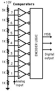
 Illustrated is a 3-bit flash ADC with resolution 1 volt (after Tocci). The resistor net and comparators provide an input to the combinational logic circuit, so the conversion time is just the propagation delay through the network - it is not limited by the clock rate or some convergence sequence. It is the fastest type of ADC available, but requires a comparator for each value of output (63 for 6-bit, 255 for 8-bit, etc.) Such ADCs are available in IC form up to 8-bit and 10-bit flash ADCs (1023 comparators) are planned. The encoder logic executes a truth table to convert the ladder of inputs to the binary number output.
Now we lets take a look at the various Analog to Digital convertors that are most commonly used with our controllers
| Name | Description |
| ADC0800 | 8-bit ADC |
| ADC0801 | 8-bit ADC 100us 0.25 LSB |
| ADC0802 | 8-bit ADC 100us 0.5 LSB |
| ADC0804 | 8-bit ADC 100us 1.0 LSB |
| ADC0808 | 8-bit 8 channel 100us ADC |
| ADC0809 | 8-Bit 8 channel ADC (=~ADC0808) |
| AD571 | 10-Bit, A/D Converter, Complete with Reference and Clock |
| MAX1204 | 5V, 8-Channel, Serial, 10-Bit ADC with 3V Digital Interface |
| MAX1202 | 5V, 8-Channel, Serial, 12-Bit ADCs with 3V Digital Interface |
| MAX195 | 16-Bit, Self-Calibrating, 10us Sampling ADC |
More information on how to interface the above listed ADC can be obtained from the datasheets of respective ICs. In the next part of tutorial we will look into the interfacing and programming of a simple 8-bit ADC (ADC0804).
ADC0804 Pinout and Typical Connections
As shown in the typica circuit, ADC0804 can be interfaced with any microcontroller. You need a minimum of 11 pins to interface ADC0804, eight for data pins and 3 for control pins. As shown in the typical circuit the chip select pin can be made low if you are not using the microcontroller port for any other peripheral (multiplexing).
There is a universal rule to find out how to use an IC. All you need is the datasheet of the IC you are working with and take a look at the timing diagram of the IC which shows how to send the data, which signal to assert and at what time the signal should be made high or low etc.
Note: Keep this in mind that whenever you are working with an IC and you want to know how to communicate with that IC, then simply look into the timing diagram of that IC from its datasheet. It gives you complete information that you need regarding the communication of IC.


The above timing diagrams are from ADC0804 datasheet. The first diagram (FIGURE 10A) shows how to start a conversion. Also you can see which signals are to be asserted and at what time to start a conversion. So looking into the timing diagram FIGURE 10A. We note down the steps or say the order in which signals are to be asserted to start a conversion of ADC. As we have decided to make Chip select pin as low so we need not to bother about the CS signal in the timing diagram. Below steps are for starting an ADC conversion. I am also including CS signal to give you a clear picture. While programming we will not use this signal.
- Make chip select (CS) signal low.
- Make write (WR) signal low.
- Make chip select (CS) high.
- Wait for INTR pin to go low (means conversion ends).
Once the conversion in ADC is done, the data is available in the output latch of the ADC. Looking at the FIGURE 10B which shows the timing diagram of how to read the converted value from the output latch of the ADC. Data of the new conversion is only avalable for reading after ADC0804 made INTR pin low or say when the conversion is over. Below are the stepts to read output from the ADC0804.
- Make chip select (CS) pin low.
- Make read (RD) signal low.
- Read the data from port where ADC is connected.
- Make read (RD) signal high.
- Make chip select (CS) high.
In the next section of this tutorial we will follow the above mentioned steps to program the ADC.
8051 Assembly Programming for ADC0804
rd equ P1.0 ;Read signal P1.0
wr equ P1.1 ;Write signal P1.1
cs equ P1.2 ;Chip Select P1.2
intr equ P1.3 ;INTR signal P1.3
adc_port equ P2 ;ADC data pins P2
adc_val equ 30H ;ADC read value stored here
org 0H
start: ;Start of Program
acall conv ;Start ADC conversion
acall read ;Read converted value
mov P3,adc_val ;Move the value to Port 3
sjmp start ;Do it again
conv: ;Start of Conversion
clr cs ;Make CS low
clr wr ;Make WR Low
nop
setb wr ;Make WR High
setb cs ;Make CS high
wait:
jb intr,wait ;Wait for INTR signal
ret ;Conversion done
read: ;Read ADC value
clr cs ;Make CS Low
clr rd ;Make RD Low
mov a,adc_port ;Read the converted value
mov adc_val,a ;Store it in local variable
setb rd ;Make RD High
setb cs ;Make CS High
ret ;Reading done
Programming 8051 in C for ADC0804
#include <REGX51.H>#define adc_port P2 //ADC Port
#define rd P1_0 //Read signal P1.0
#define wr P1_1 //Write signal P1.1
#define cs P1_2 //Chip Select P1.2
#define intr P1_3 //INTR signal P1.3
void conv(); //Start of conversion function
void read(); //Read ADC function
unsigned char adc_val;
void main(){
while(1){ //Forever loop
conv(); //Start conversion
read(); //Read ADC
P3 = adc_val; //Send the read value to P3
}
}
void conv(){
cs = 0; //Make CS low
wr = 0; //Make WR low
wr = 1; //Make WR high
cs = 1; //Make CS high
while(intr); //Wait for INTR to go low
}
void read(){
cs = 0; //Make CS low
rd = 0; //Make RD low
adc_val = adc_port; //Read ADC port
rd = 1; //Make RD high
cs = 1; //Make CS high
}
Pulse Width Modulation
Pulse width Modulation or PWM is one of the powerful techniques used in control systems today. They are not only employed in wide range of control application which includes: speed control, power control, measurement and communication. This tutorial will take you through the PWM basics and implementation of PWM on 8051.
Basic Principal of PWM
Pulse-width Modulation is achived with the help of a square wave whose duty cycle is changed to get a varying voltage output as a result of average value of waveform. A mathematical explanation of this is given below.
Consider a square wave shown in the figure above.
Ton is the time for which the output is high and Toff is time for which output is low. Let Ttotal be time period of the wave such that,

Duty cycle of a square wave is defined as 
The output voltage varies with duty cycle as...

So you can see from the final equation the output voltage can be directly varied by varying the Ton value.
If Ton is 0, Vout is also 0.
if Ton is Ttotal then Vout is Vin or say maximum.
This was all about theory behind PWM. Now lets take a look at the practical implementation of PWM on microcontrollers.
The basic idea behind PWM implementation on 8051 is using timers and switching port pin high/low at defined intervals. As we have discussed in the introduction of PWM that by changing the Ton time, we can vary the width of square wave keeping same time period of the square wave.
We will be using 8051 Timer0 in Mode 0. Values for high and low level will be loaded in such a way that total delay remains same. If for high level we load a value X in TH0 then for low level TH0 will be loaded with 255-X so that total remains as 255.
Timer setup for PWM
PWMPIN EQU P1.0 ; PWM output pin
PWM_SETUP:
MOV TMOD,#00H ; Timer0 in Mode 0
MOV R7, #160 ; Set pulse width control
; The value loaded in R7 is value X as
; discussed above.
SETB EA ; Enable Interrupts
SETB ET0 ; Enable Timer 0 Interrupt
SETB TR0 ; Start Timer
RET
Interrupt Service Routine
TIMER_0_INTERRUPT:
JB F0, HIGH_DONE ; If F0 flag is set then we just finished
; the high section of the
LOW_DONE: ; cycle so Jump to HIGH_DONE
SETB F0 ; Make F0=1 to indicate start of high section
SETB PWMPIN ; Make PWM output pin High
MOV TH0, R7 ; Load high byte of timer with R7
; (pulse width control value)
CLR TF0 ; Clear the Timer 0 interrupt flag
RETI ; Return from Interrupt to where
; the program came from
HIGH_DONE:
CLR F0 ; Make F0=0 to indicate start of low section
CLR PWMPIN ; Make PWM output pin low
MOV A, #0FFH ; Move FFH (255) to A
CLR C ; Clear C (the carry bit) so it does
; not affect the subtraction
SUBB A, R7 ; Subtract R7 from A. A = 255 - R7.
MOV TH0, A ; so the value loaded into TH0 + R7 = 255
CLR TF0 ; Clear the Timer 0 interrupt flag
RETI ; Return from Interrupt to where
; the program came from
In your main program you need to call this PWM_SETUP routine and your controller will have a PWM output. Timer Interrupt service routine will take care of PWM in the background. The width of PWM can be changed by changing the value of R7 register. In above example I am using 160, you can choose any value from 0 to 255. R7 = 0 will give you o/p 0V approx and R7 = 255 will give you 5V approx.
You can also make use of Timer1 if you want. And the output pin can be changed to whatever pin you want.
Timer setup for PWM in C
//Global variables and definition
#define PWMPIN P1_0
unsigned char pwm_width;
bit pwm_flag = 0;
void pwm_setup(){
TMOD = 0;
pwm_width = 160;
EA = 1;
ET0 = 1;
TR0 = 1;
}
Interrupt Service Routine
void timer0() interrupt 1 {
if(!pwm_flag) { //Start of High level
pwm_flag = 1; //Set flag
PWMPIN = 1; //Set PWM o/p pin
TH0 = pwm_width; //Load timer
TF0 = 0; //Clear interrupt flag
return; //Return
}
else { //Start of Low level
pwm_flag = 0; //Clear flag
PWMPIN = 0; //Clear PWM o/p pin
TH0 = 255 - pwm_width; //Load timer
TF0 = 0; //Clear Interrupt flag
return; //return
}
}
UART Programming and MAX232 Interfacing
UART (Universal Asynchronous Receiver Transmitter) or USART (Universal Synchronous Asynchronous Receiver Transmitter) are one of the basic interface which you will find in almost all the controllers available in the market till date. This interface provide a cost effective simple and reliable communication between one controller to another controller or between a controller and PC.
RS-232 Basics
RS-232 (Recommended Standard 232) is a standard for serial binary data signals connecting between a DTE (Data terminal equipment) and a DCE (Data Circuit-terminating Equipment).
Voltage Levels:
The RS-232 standard defines the voltage levels that correspond to logical one and logical zero levels. Valid signals are plus or minus 3 to 25 volts. The range near zero volts is not a valid RS-232 level; logic one is defined as a negative voltage, the signal condition is called marking, and has the functional significance of OFF. Logic zero is positive, the signal condition is spacing, and has the function ON.
So a Logic Zero represented as +3V to +25V and Logic One represented as -3V to -25V.

RS-232 Level Converters
Usually all the digial ICs works on TTL or CMOS voltage levels which cannot be used to communicate over RS-232 protocol. So a voltage or level converter is needed which can convert TTL to RS232 and RS232 to TTL voltage levels.
The most commonly used RS-232 level converter is MAX232. This IC includes charge pump which can generate RS232 voltage levels (-10V and +10V) from 5V power supply. It also includes two receiver and two transmitters and is capable of full-duplex UART/USART communication.
MAX232 Interfacing with Microcontrollers
To communicate over UART or USART, we just need three basic signals which are namely, RXD (receive), TXD (transmit), GND (common ground). So to interface MAX232 with any microcontroller (AVR, ARM, 8051, PIC etc..) we just need the basic signals. A simple schematic diagram of connections between a microcontroller and MAX232 is shown below
8051 Programming for UART
In 8051, we make use of Timer 1 to generate the required baud rate. Following are the registers that are need to be configured to commnunicate over UART.
TMOD: This register is used to set the mode of Timer0 and Timer1. It is also used to select whether the timers are used as Timer or Counter.
SCON: Serial Control register has various functions like.. it has flags for Framing error, Transmit interrup and receive interrupt. Its used to select the serial port mode, to enable or disable the reception etc.
TCON: This register has varios flag and control bits e.g. Timer overflow flags, interrupt edge flags, timer control bits to start/stop the timer.
TH1 & TL1: Timer registers for Timer 1 determines the baudrate of UART.
More information on the above registers can be found in the 8051 Hardware manual.
Initializing USART in 8051
Serial_Init:
;Set timer 1 mode to 8-bit Auto-Reload
mov TMOD,#20H
;Enable reception
;Set Serial port mode to 8-bit UART
mov SCON,#50H
;Set baudrate to 9600 at 11.0592MHz
mov TH1,#0FDH
mov TL1,#0FDH
;Start Timer
setb TR1
ret
in C we can do this as..
#include <reg51.h>.
void serial_init(){
TMOD = 0x20;
SCON = 0x50;
TH1 = 0xFD;
TL1 = 0xFD;
TR1 = 1;
}
To Send data to the serial port we just have to move the data in SBUF (serial buffer register) and wait for the Transmit Interrupt flag to be set. While receiving we wait for the Receive interrupt flag to be set and read the data from SBUF register. This can be done as shown below...
Serial_Send:
;wait for last data to be
;sent completely
jnb TI,Serial_Send
;clear the transmit interrupt flag
clr TI
;Then move the data to send in SBUF
mov SBUF,A
ret
Serial_Read:
;Wait for Receive interrupt flag
jnb RI,Serial_Read
;If falg is set then clear it
clr RI
;Then read data from SBUF
mov A,SBUF
ret
or in c as
void serial_send(unsigned char dat){
while(!TI);
TI = 0;
SBUF = dat;
}
unsigned char serial_read(){
while(!RI);
RI = 0;
return SBUF;
}